 On-wafer Measurement Facility
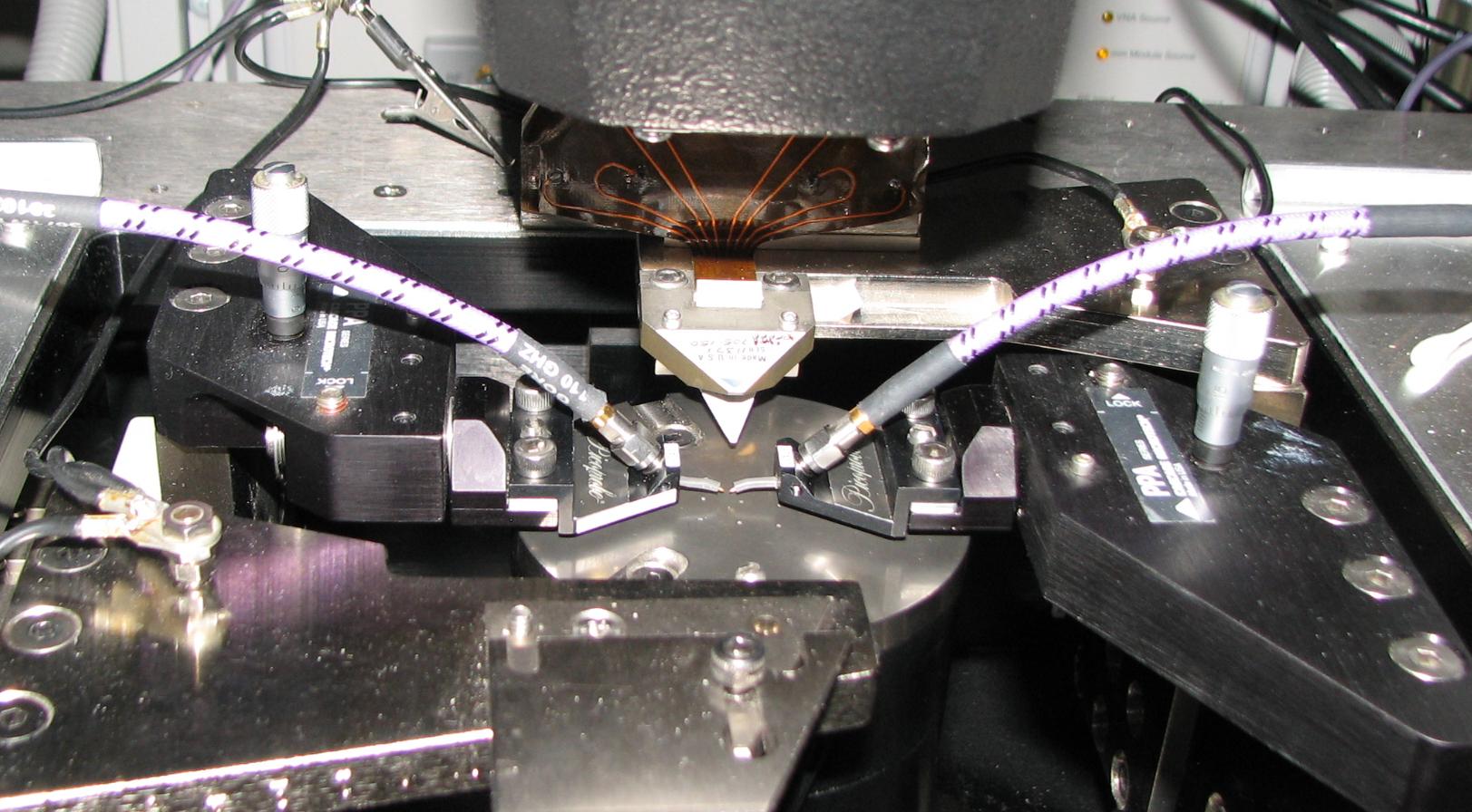
On-wafer measurements are becoming increasingly important in the microwave electronics. Modern integrated circuit designs have opened the way to extreme miniaturization in enabling high levels of integration in both scientific and commercial applications. The measurement facility at the DTU Electrical Engineering, offers accurate characterization of integrated circuits in a frequency range from DC to 110 GHz. Two Wafer Probe Stations available for IC probing are actively used for on-wafer characterization of various circuits designed at the Department. This includes microwave and millimeter-wave low-noise amplifiers, active and passive mixers, frequency multipliers, voltage controlled oscillators, reflective and non-reflective switches, millimeter-wave power amplifiers, passive circuits, and many others. The facility utilizes spectrum analyzers, oscilloscopes, power meters and vector network analyzer with over a hundred gigahertz bandwidth.
 Radio Anechoic Chamber
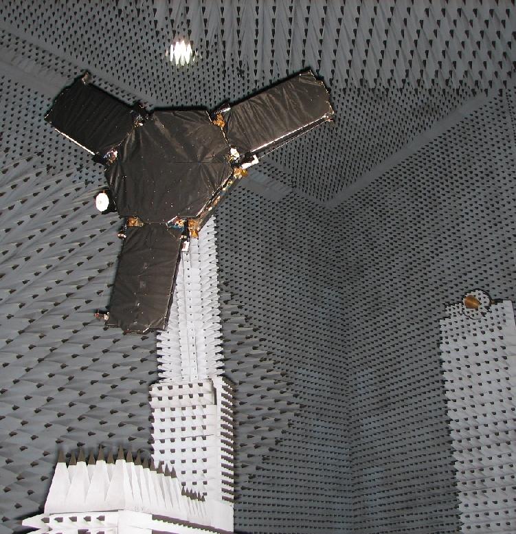
The Radio Anechoic Chamber at DTU Electrical Engineering is an essential part of the DTU-ESA antenna measurement facility. The anechoic chamber is recognized throughout Europe for high quality measurements and regularly used for accurate characterization and calibration of various antennas for ESA space missions as well as for Danish and European companies. The antenna measurement facility is actively exploited in department's research projects and teaching activities.
Detailed information is available on the dedicated DTU-ESA web-page.
Ground Penetrating Radar Lab
Education
EMI Lab
The EMI laboratory is maintained by Electromagnetic Systems Research Group and is actively used by students in a number of university courses, master and bachelor projects. It is organized in seven distinctive work-places, where students conduct measurements and experiments, using newly aquired modern equipment. Among the equipment used includes vector network analyzers, signal generators, digital oscilloscopes, spectrum analyzers, multimeters and many other complex technical instruments.
Satellite Communications Lab
Fabrication
 Workshop
The workshop is hosted by the Electromagnetic Systems Research Group, and shared with the Department of Photonics Engineering and the Division of Microwaves and Remote Sensing. The workshop encourages experimental activities by providing custom designs, fabrication and assembling of various mechanical parts.
The workshop offers moreover high precession machinery used actively for fabrication of high performance electromagnetic structures.
 Thin Film Laboratory
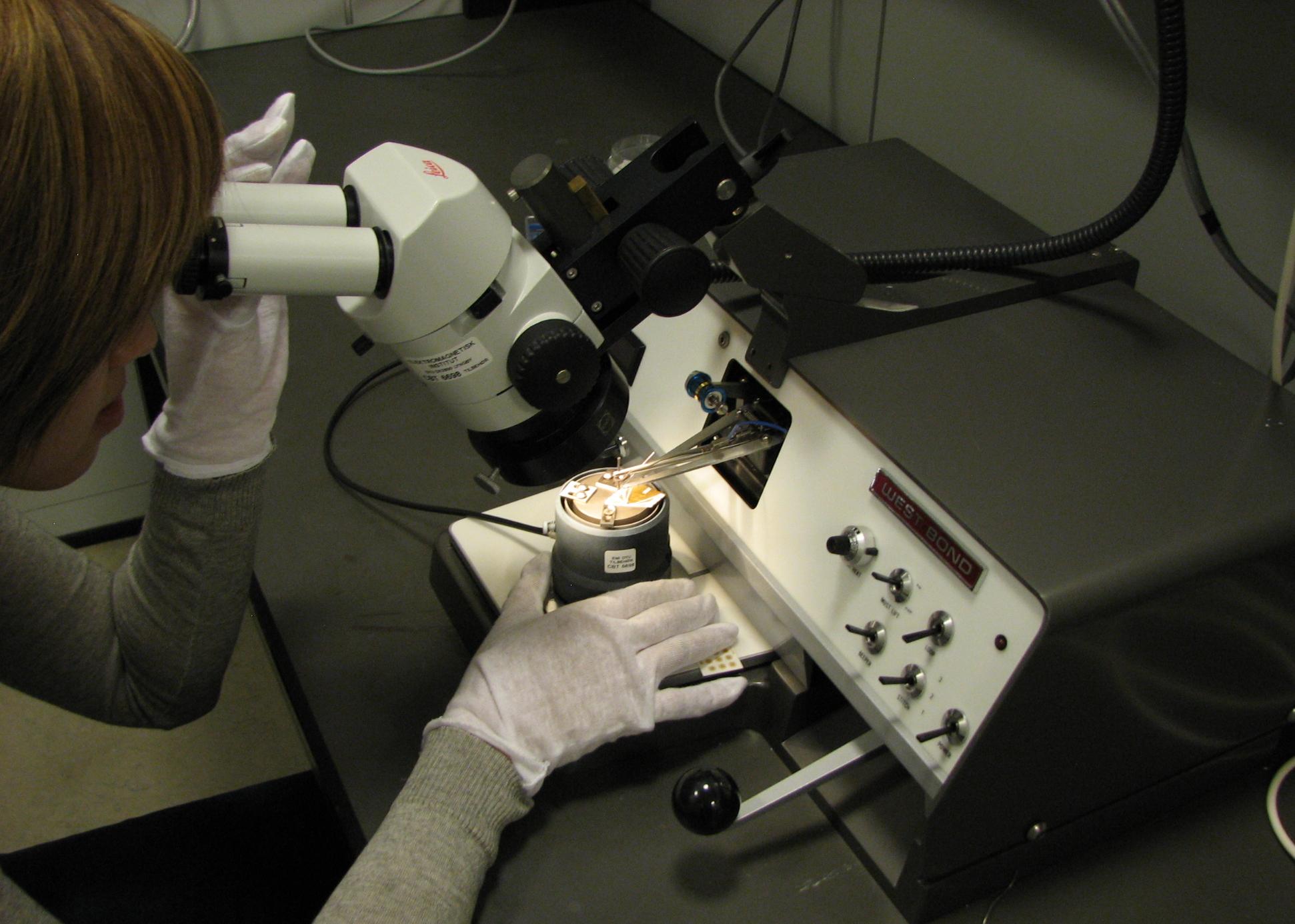
Our thin film laboratory is mostly oriented for post-processing of dies. The laboratory is generally used for visual examination of integrated circuits (using a dedicated microscope) and mounting them on a supporting substrate which is followed by a bounding in the semi-clean room.
The facility is equipped with two Memmert ovens for in-house processing of low temperature co-fired ceramic (LTCC) devices.
 Thick Film Laboratory
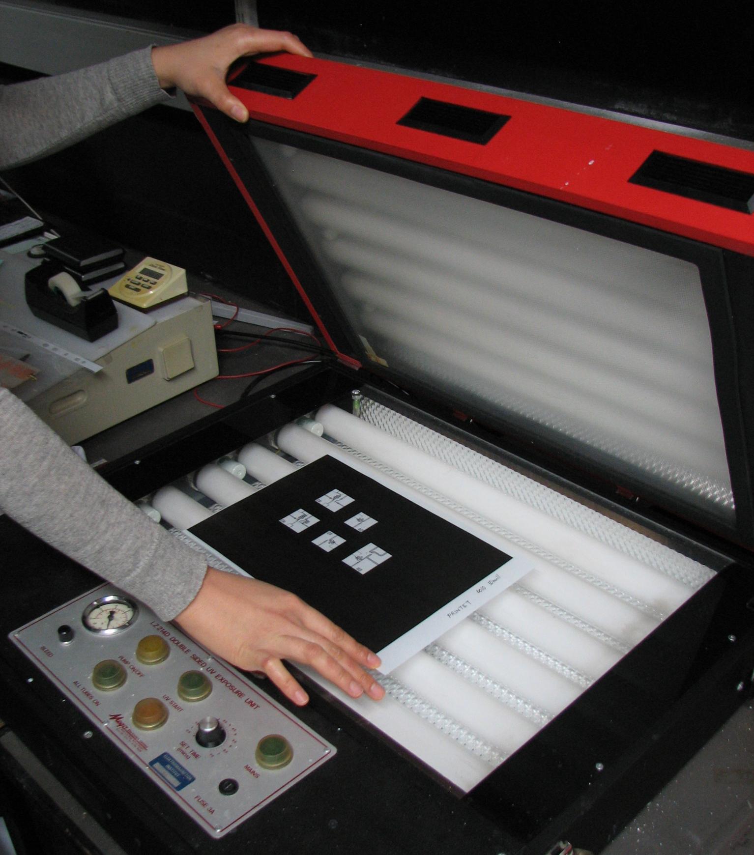
Our thick film laboratory serves for fabrication of printed circuit boards based on various substrate materials. It is equipped with two double sided exposure units for processing single and double sided planar structures and allowing pattern fabrication an accuracy better than 0.1 mm.
The facility is actively used for manufacturing of microstrip devices and planar antennas for students as well as for external projects.
 Semi-clean Room
The semi-clean room complements our thin film laboratory and serves for post-processing of dies. It is equipped with a bounding machine and provides an environment for handling fragile semiconductor solid-state structures.
For further questions please contact Olav Breinbjerg.